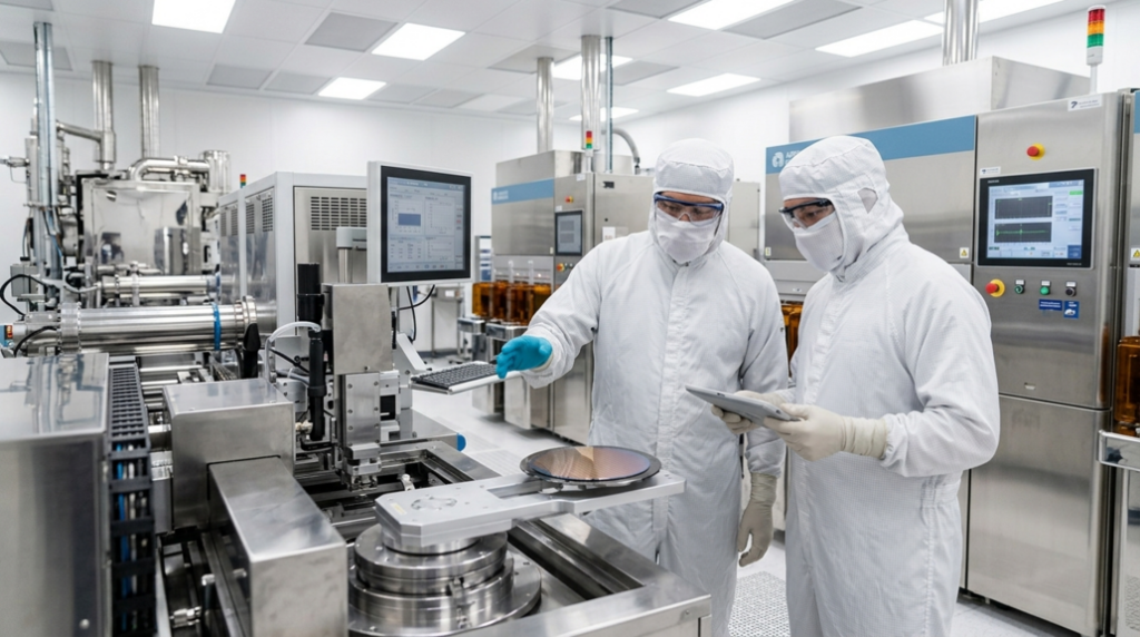
Applied Materials officially opened its Equipment and Process Innovation and Commercialization (EPIC) Center in Sunnyvale, California, marking a $5 billion investment to establish the world’s largest dedicated semiconductor research and development facility. The center, unveiled in October 2026, covers approximately 600,000 square feet, including nearly four acres of advanced cleanroom space designed for process and equipment innovation.
The EPIC Center aims to expedite the journey from semiconductor materials research to high-volume manufacturing, reducing typical development cycles. This acceleration addresses the growing demand for AI processors, memory chips, and other next-generation semiconductor technologies.
Applied Materials developed the EPIC Center in collaboration with leading chipmakers such as TSMC, Intel, SK hynix, Micron, Samsung Electronics, as well as various equipment companies and academic partners. This collaborative environment is intended to foster quicker innovation cycles and strengthen the U.S. semiconductor industry’s competitiveness at a time of global supply chain challenges and strategic technological importance.
Situated at Applied Materials’s Sunnyvale campus near the company’s headquarters, the facility represents the company’s largest-ever capital expenditure and reflects an increasing commitment to domestic semiconductor manufacturing capabilities. Industry experts view the facility as a significant step toward enhancing American capacity for advanced semiconductor production and innovation.